- 您现在的位置:买卖IC网 > Sheet目录287 > 24LC01B-I/SNG (Microchip Technology)IC EEPROM 1KBIT 400KHZ 8SOIC
24AA01/24LC01B
2.0
PIN DESCRIPTIONS
The descriptions of the pins are listed in Table 2-1.
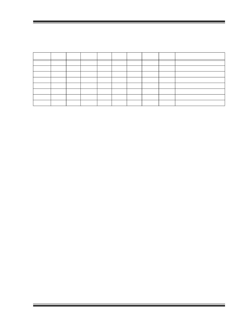
TABLE 2-1:
PIN FUNCTION TABLE
Name
A0
A1
A2
V SS
SDA
SCL
WP
V CC
PDIP
1
2
3
4
5
6
7
8
SOIC
1
2
3
4
5
6
7
8
TSSOP
1
2
3
4
5
6
7
8
DFN
1
2
3
4
5
6
7
8
TDFN
1
2
3
4
5
6
7
8
MSOP
1
2
3
4
5
6
7
8
SOT23
—
—
—
2
3
1
5
4
SC-70
—
—
—
2
3
1
5
4
Description
Not Connected
Not Connected
Not Connected
Ground
Serial Address/Data I/O
Serial Clock
Write-Protect Input
+1.7V to 5.5V Power Supply
2.1
A0, A1, A2
2.3
Serial Clock (SCL)
The A0, A1 and A2 pins are not used by the 24XX01.
They may be left floating or tied to either V SS or V CC .
The SCL input is used to synchronize the data transfer
to and from the device.
2.2
Serial Address/Data Input/Output
2.4
Write-Protect (WP)
(SDA)
The SDA input is a bidirectional pin used to transfer
addresses and data into and out of the device. Since
it is an open-drain terminal, the SDA bus requires a
pull-up resistor to V CC (typical 10 k Ω for 100 kHz,
2 k Ω for 400 kHz).
For normal data transfer, SDA is allowed to change
only during SCL low. Changes during SCL high are
reserved for indicating Start and Stop conditions.
? 2009 Microchip Technology Inc.
This pin must be connected to either V SS or V CC .
If tied to V SS , normal memory operation is enabled
(read/write the entire memory 00-7F).
If tied to V CC , write operations are inhibited. The entire
memory will be write-protected. Read operations are
not affected.
DS21711J-page 5
发布紧急采购,3分钟左右您将得到回复。
相关PDF资料
24LC024H-I/ST
IC EEPROM 2KBIT 400KHZ 8TSSOP
24LC025T-E/MC
IC EEPROM 2KBIT 400KHZ 8DFN
24LC04B-E/P
IC EEPROM 4KBIT 400KHZ 8DIP
24LC04BH-E/P
IC EEPROM 4KBIT 400KHZ 8DIP
24LC08BH-E/P
IC EEPROM 8KBIT 400KHZ 8DIP
24LC1025-E/P
IC EEPROM 1MBIT 400KHZ 8DIP
24LC16BH-E/P
IC EEPROM 16KBIT 400KHZ 8DIP
24LC21-I/P
IC EEPROM 1KBIT 400KHZ 8DIP
相关代理商/技术参数
24LC01B-I/ST
功能描述:电可擦除可编程只读存储器 128x8 - 1.8V RoHS:否 制造商:Atmel 存储容量:2 Kbit 组织:256 B x 8 数据保留:100 yr 最大时钟频率:1000 KHz 最大工作电流:6 uA 工作电源电压:1.7 V to 5.5 V 最大工作温度:+ 85 C 安装风格:SMD/SMT 封装 / 箱体:SOIC-8
24LC01B-I/STG
功能描述:电可擦除可编程只读存储器 128x8 - 1.8V Lead Free Package
RoHS:否 制造商:Atmel 存储容量:2 Kbit 组织:256 B x 8 数据保留:100 yr 最大时钟频率:1000 KHz 最大工作电流:6 uA 工作电源电压:1.7 V to 5.5 V 最大工作温度:+ 85 C 安装风格:SMD/SMT 封装 / 箱体:SOIC-8
24LC01BIOT
制造商:Microchip Technology Inc 功能描述:
24LC01BIP
制造商:Panasonic Industrial Company 功能描述:IC
24LC01BMODULES
制造商:MICROCHIP 制造商全称:Microchip Technology 功能描述:1K/2K I2C Serial EEPROMs in ISO Micromodules
24LC01B-MT
制造商:MICROCHIP 制造商全称:Microchip Technology 功能描述:1K/2K I 2 C ⑩ Serial EEPROMs in ISO Micromodules
24LC01BP
制造商:MICRO CHIP 功能描述:*
24LC01BSN
制造商:MICRO CHIP 功能描述:New
